CENG 4354: Digital System Design
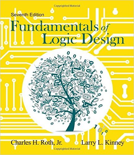
 Charles H. Roth, Jr., Cengage Learning, "Fundamentals of Logic Design", 7th
Edition, 2014. Publisher: CL Engineering, 2013. ISBN-10: 1133628478, ISBN-13:
978-1133628477.
References: Sudhakar Yalamanchili, "Introductory VHDL: From Simulation to
Synthesis," 1st edition, Publisher: Pearson, 2000. ISBN-10: 0130809829,
ISBN-13: 9780130275684.
Many web references, hands-on training materials, VHDL design examples.
Course slides will be available for download on the blackboard.
VIM Editor (Optional) ModelSim Altera Starter Edition (Mandatory) Mentor Graphic Modelsim PE Student Edition (Mandatory)
Overall goal: study the process and basic knowledge of designing an applications-specific integrated circuit (ASIC) or field-programming gate array (FPGA), focusing on the front-end IC design flow..
CENG 3312 (Digital Circuits)
Prepare the basic hardware description language (HDL) design knowledge for future chip design engineer in semiconductor industry or VLSI/IC research; example companies in job market include Intel, AMD, Qualcomm, and Apple etc.
Introduction to industrial IC design flow Combinational and sequential logic design with VHDL Finite State Machine and Data Path Design (Floating-point to fiexed-point conversion) Resource cost and timing constrains in integrated circuit (IC) design Design performance with resource cost, speed, and power Project-driven study, including HDL design and basic simulation environment (Design-Under-Test/testbench/monitor/script)
Upon completion of this course, students will be able to: know the most recent industrial AISC/FPGA design flow (floating-point to fixed-point conversion, HDL design, verification, synthesis, layout/placement and route) know the latest ASIC/FPGA design tools provided by industrial vendors like Synopsys, Cadence, Mentor Graphic; and Xilinx and Altera describe the operation and timing constraints for latches and registers draw a basic sequential circuit diagram and analyze its timing properties (propagation delays, setup and hold times, clock-q delay, clock skew, and the minimum clock period). evaluate digital systems using various metrics: the maximum operational frequency (MOF) and throughput, gate/slice count and area, power and energy dissipation. using VHDL, design a basic system-on-chip (SoC) involving data-path and finite state machine (FSM) on an FPGA learn how to write test-benches and perform verification of the digital system employ ASIC/FPGA design tools (front-end) and script, including Vim editor, tcl script, and ModelSim simulator
Lec1: Syllabus, Industrial ASIC and FPGA Design Flow (SYch1) Lec2: Digital System (SYch2 and ch3) Lec3: VHDL for Combinational Logic (SYch4, SYch5) Lec4: Introduction to VHDL (ch10) and EDA Tool Training: ModelSim Simulation (Training) Lec5: Analysis of Clocked Sequential Circuits (ch13) Lec6: Derivation of State Graphs and Tables (ch14) Lec7: Reduction of State Tables State Assignment (15) Lec8: Sequential Circuit Design (ch16) Lec9: Circuit for Arithmetic Operations -- Approximate Design (ch18) Lec10: State Machine Design with SM Charts (ch19) Lec11: VHDL for Sequential Logic and Digital System Design (ch17 & ch20) Lec12: VHDL for Sequential Circuit (SYch6: 6.1~6.2, 6.4, 6.7~6.10) Lec13: VHDL for Sequential Circuit Cont. (SYch7: 7.1,7.2,7.7,7.8)